Animation of Formation of a Depletion Layer at the Junction
of Two Semiconductors
Introduction
We will
need to animate phonons of a crystal as well as the collisions of electrons
with the charge centers of the vibrating nuclei associated with the phonons. These collisions impede the drift in an
electric field, as well as the diffusion, of electrons and holes. When the p side of the junction is brought
into contact with the n side, holes start to diffuse from the p side into the n
side leaving bare negative ions in the p side as well as a net positive charge
on the n side. Similarly, electrons
start to diffuse from the n side into the p side leaving bare positive ions in
the n side as well as a net negative charge on the p side. After sufficient
diffusion time, the diffusion is halted due to this buildup of opposite charge
density on each side of the junction. This charge density leads to an electric
potential distribution (Vbuilt in) that opposes the flow of more holes
and electrons. When a sufficient electric
potential of the appropriate sign is applied across the junction, the potential
distribution is overcome and electrons and holes are able to flow again. This latter behavior will also be animated.
Figures:

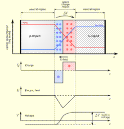
Figure 0:The "standard"
model of the charge distribution,
electric field E, and voltage V Vs position for a p-n junction.

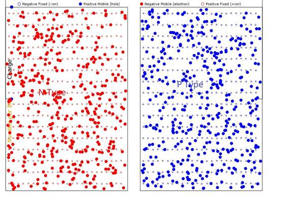
Figure 1. pn junction before fusing All charge types are color-coded. Please read the codes.

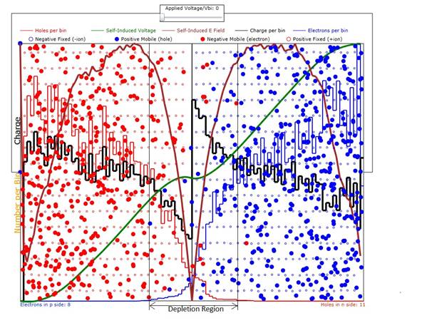
Figure 2. pn junction after fusing. The depletion region is labeled at the bottom
of the Figure. All curves and charge
types are color-coded. Please read the
codes.
Calculations
1. Calculation of the voltage Vs position in
the junction area
The voltage is obtained by the Poisson equation in one
dimension as:
(1)
where ε is the dielectric constant and ρ(x) is
the charge distribution. Note that ρ does not depend on y and z. If
the variation of ρ is as follows:
(2)
where 2d is the total width of the depletion region and the
units of ρ1 are coulombs per meter
cubed so that the sheet charge density is ρ1d for each of the two parts
of the depletion layer.
Then the solution for x component of the electric field is
while the electric field in the y and z direction is zero.
(3)
We can further integrate E(x) to obtain V(x):
(4)
where V(0)=0 has been chosen.
For a more general sheet-like charge distribution, σ (coulombs m-2), we can suppose a charge of small thickness
d1, centered at -/+ d/2. Let the total charge in the sheet be the
same as before
and, to start, center σ at x=-/+d/2.
The resulting peak E field is the same as for the thick charge
The potentials at -/+ infinity, for the case where the
charged layers are centered at -/+ d/2 are the same as before:
To compute the fields for an arbitrary distribution of
charge, we can use superpositions of charged layers like σ. Note that the peak electric field for σ doesn't
depend on the spacing of the charged layers but the potentials at -/+infinity are linearly proportional to layer
spacing. For example
where the two layers are centered at x=-/+d2.
In order to compute the electric field due to a large group
of layers of thickness d1 we use the following summation:
where the layers are centered at positions xi,
separated uniformly by dx, and xj is an observation coordinate
greater than xi.
Similarly to obtain the potential at xj we use
the following summation:
2. Electron/Hole Velocity Response to Potentials
The electron (e) and hole (h) velocities are changed as they
traverse the electric potential due to depleted layer. Both e and h have the x component of their
velocities reduced when they climb their respective potential energy barriers Ue(x)
and Uh(x) where
where e is the elementary charge and is here considered to
be positive.
Using Newton's
law to compute the velocity change per time increment we have:
where, t is time and mh and me are the
masses of h and e particles, respectively.
Of course, the electron's progress into the p region is with
a negative vx and its vx is incremented as it climbs its
potential hill thereby reducing its rate of progress into the p region. The result of all this is that, in steady
state, there are very few h in the n region and very few e in the p region.
3. Electron-Lattice Collisions
While the
correct way to handle these collisions is a wavelike treatment using the
quantum description of electron wave and phonon waves in the crystal, for
simplicity here we will use hard sphere collisions between the electrons/holes
(e/h) and the much more massive nuclei at the lattice points of the crystal. That way the thermally excited lattice will
impede the diffusion of the e/h particles as is usually expected from
electron-phonon collisions.
Since the nuclei are much more massive than the e/h
particles, we will assume that no energy or momentum is given up to the
nuclei. If the location of the e/h is at
(x1,y1,z1) and the nucleus is at (x2,y2,z2),
then a unit vector pointing from the e/h to the nucleus is
(5)
where
Thus the only thing that happens to the e/h is to reverse
the component of its momentum along the u
direction. The new (denoted by prime) velocity
vector becomes:
(6)
where, by taking the dot product of u times both sides of the equation, it can easily be shown that
as required.
4. What the Program Calculates
The program computes the position, taking into account the
electric field forces and lattice scattering, of all of the mobile carriers
(electrons and holes) and sums these in horizontal-axis-correlated (xi)
bins. Since we have a rather low number
of carriers per bin, the program sums the number at the ith bin so that what is
plotted and used is really the average number of carriers per bin over a long
period of time. Since equilibrium is
always reached, this averaging does not affect the results. The program then sums the charges (of both
mobile and fixed charges) at each of the bins and plots the result. This charge distribution is then used to
compute the built-in voltage and electric field distribution as discussed in Section
1 above. The resulting electric field
distribution is used, along with the collision dynamics from Section 3, to
compute the motion of the charges as discussed above in Section 2.
When a
forward bias is applied across the pn junction, the built-in voltage is
partially cancelled and the electric field that repels motion of the carriers
is reduced so that current can flow.
Since the carrier density is lowest at the interface (and therefore the
resistivity is highest there) most of the electric field reduction occurs near
this interface. When the field at the
interface becomes positive, current flows through the pn junction and is
depicted by having red electrons flow through the voltage source.
Summary
This has
been a demonstration of the power of using simulation of a relatively small
number of carriers to get a more heuristic view of some very complicated
processes in a simple semiconductor device.
