This document will show how to compute the single electron energy band gap of a solid crystal. The most important material in our present "information age" technology is a semiconductor and its importance stems from the existence of its electron energy band gap. In a pure semiconductor crystal, the electrons are confined at zero temperature to a lower energy condition called the valence band. The higher enerrgy electron conduction band is separated from the valence band by an energy gap called the band gap. If the semiconductor is to be useful for a device, the band gap must be large enough that the electrons' thermal energy is not enough to easily promote the electrons into the conduction band and small enough that the thermal promotion can provide enough promotion when needed. Germanium, which was the first semiconductor device material to be used is an example of a material whose band gap is too small (0.67 electron volts) to be used in engine computers which have to perform in temperatures above 100 Celsius. On the other hand, crystal quartz which is classed as an insulator with a band gap of 9.65 electron volts cannot be used in a semiconductor device because normal temperatures do not allow enough thermal promotion to the conduction band. A much more useful semiconductor for devices is silicon with a band gap of 1.14 electron volts. This band gap is large enough to avoid thermal reverse current in diodes and transistors but small enough to achieve large forward bias current when needed. Silicon is the material of choice for almost all computer chips. In addition to being used in computer chips which are usually binary devices, semiconductors are used in transistors which can amplify signals like needed in a radio, light emitting diodes (LEDs), solar panels, and laser diodes. The band gap of semiconductors is important because it helps to provide the electrical current directional asymmetry in diodes and transistors. When an n doped region is fused to a p doped region semiconductor to make a diode or transistor, a builtin voltage, `V_(bi)`, is developed. This voltage is proportional to, and somewhat smaller than, the band gap of the semiconductor. When a votage is applied `V_(bi)` permits large current flow in the forward direction and almost no current flow in the reverse direction. `V_(bi)` which is dependent on the band gap, is what allows us to make semiconductor devices. For a discussion of the calculation of the `V_(bi)` see the Appendix at the end of this document.
In a solar panel, which is a string of diodes open to the sun, photons from the sun promote electrons from the valence band to the conduction band which results in a voltage approximately equal in electron volts to the band gap across the solar panel diode. When the two sides of the diod are connected through a load, a current flows and the current provides energy to the load.
Light emitting diodes (LEDs) are the reciprocal of solar panels. In a LED, the applied forward voltage causes demotion of an electron to the valence band along with the emission of a photon whose energy is approximately equal to the band gap.
It will be sufficient to compute the band gap that a single electron experiences. Since the crystal has no net charge (charge neutral) except for the single electron, the many other electrons are confined around their nucleii which are equally spaced.
Therefore, we can model the stationary atoms as nucleii surrounded by electron charge clouds. For our single electron, the electron charge cloud represents a repulsive force since the positive nucleus will usually be much farther away than the electron cloud. Since the atoms are spaced periodically, it will be sufficient to model their atom potentials as a cosine function. Each of these charge centers will seem like slightly negative ions to our single electron. To behave like a solid we need one other property: a much larger repulsive potential at its boundaries to keep the single free electron from escaping. This potential is called the work function. In the photoelectric experiment whose explanation won the Nobel prize for Albert Einstein, the photon enegy needed to eject an electron from the photocell was equal to the work function. So for our calculation we will assume the boundaries are those of a "square well" and then the potential energy that we use in the Schrodinger wave equation is what is called a "finite square well" with the atom array cosine potential at the bottom of the well (see Canvas 1). The total domain of the potential energy needs to be significantly larger than the width of the well to keep the electrons from tunneling through the outer walls.
It will be sufficient to compute the band gap in just one (x) dimension since each of the other two dimensions lead to the analogous result. Also we need many periodic atoms in order to see the functional form of the electron energy mode levels leading up to the band gap and receding away from it.
Here we will define a finite difference matrix of the Schrodinger equation that has a potential composed of a finite square well and a cosine function that represents the potentials due to ions in a linear chain of atoms. The potential is therefore defined as
`V(|x|)=if(|x|>w) \ then \ V=V_(outside) \ else \ V=V_(cos)(k_c|x|)`
where `2w` is the width of the square well, `V_(outside)` is the depth of the square well, V_c is the height of the cosine potential and `k_c=(2pi)/a` is the wave vector of the cosine potential. In order to avoid particle tunneling through the outer walls of the square well, the total domain width will be `4w`. Then,for `n+1` data points, the array of x values will be`x[i]=[-L,-L+dx,-L+i*dx...L-(n-1)dx,L]`
where `L=(4w)/2` and `dx=(2L)/n` This data results in the potential, `V(x_i)` shown in Canvas 1.We use the potential, `V`, in the finite difference matrix that represents the time independent Schrodinger equation shown below:
` [[1/dx^2+V(x_1),-1/(2dx^2),0,0,0,0], [-1/(2dx^2),1/dx^2+V(x_2),-1/(2dx^2),0,0,0], [0,-1/(2dx^2),1/dx^2+V(x_3),-1/(2dx^2),0,0], [0,0,-1/(2dx^2),1/dx^2+V(x_4),-1/(2dx^2),0], [0,0,0,-1/(2dx^2),1/dx^2+V(x_5),-1/(2dx^2)], [0,0,0,0,-1/(2dx^2),1/dx^2V(x_6)]]((psi_1),(psi_2),(psi_3),(psi_4),(psi_5),(psi_6))-E ((psi_1),(psi_2),(psi_3),(psi_4),(psi_5),(psi_6))=0 `
where `psi_i` are the elements of the eigenvectors (wave function) and `E` is the eigenvalue (energy) for that eigenvector. The number of eigenvalues and eigenvectors that we must calculate is the same as the number of `x_i` values.The inputs are called sliders which allow the learner to adjust the Potential function. The Scrodinger solutions (eigensystem, eigenvalues and eigenvectors) are completely determined by the chosen potential function. The potential variables are
1. Number of points to describe the potential. The number of potential points is the same as the dimension of the squre finite difference matrix. This means that the number of eigenvalues and eigenvectors calculated will also be this number.
2. Width of the finite potential well which confines the particles
3. Number of Ions (N) which induce the cosine potential energy at the bottom of the finite square well. This number determines the mode number (or, equivalently, the k vector) at which the band gap occurs
4. Amplitude of the cosine potential energy function at the bottom of the finite square well. The maximum value of this amplitude is much less than the depth of the finite square well.
Canvas 0 shows a message related to the start of the mode energy calculations. It refers to the large button just above it. The cursor should change to a hand before the button is pressed. If it has not changed to a hand, please press the large button again
When this large button is alternately blinking red then black, the calculation has not yet started-press again if needed. When the blinking stops, the calcuation is proceeding
It usually takes 5 to 10 seconds to compplete.
After that the results are plotted in Canvases 2, 3, and 4.Canvas 1 displays the potential function used for the Schrodinger equation. It shows the large potentials at the left and right of the potential well and the smaller amplitude cosine variation potential at the bottom of the well. The period of cosine potential is a and is clearly labeled. The amplitude and the number of the cosine cycles are adjustable using sliders. The width of the deep finite potential well is also adjustable as are the number of points that define the potential. The latter number is also the number of energy modes that will be computed. For clarity, however, only about one fourth of the mode energies will be displayed.
Canvas 2 shows a plot of the wave mode energies. Each mode is displayed as a small circle with the mode number above the circle. The total number of modes available is the same as the number of points describing the potential. For clarity only about one fourth of the mode energies are displayed. In one dimension, mode k vectors are separated by `deltak=pi/(Na)` so the k vector vector value of the abscissa of the mode plot is just `(Mpi)/(Na)` where `N` is the number of cosine cycles inside the potential well. Then since M=N at the band gap, `k` at the gap occurs at `k=pi/a`.
By clicking on the mode circle its vector will be displayed in Canvas 3 along with the same potential function that waa displayed in Canvas 1. The band gap occurs at a mode number which corresponds to the number of cycles of the cosine potential. The splitting due to the band gap is the same as the amplitude of the cosine potential. For comparison below is a drawing of the shape of the energy function Vs k-wave vector(same as mode number) Not the retuction of slope as the mode number or k vector nears the band gap and the corresponding slope reduction just to the right of the band gap. When the cosine potential has zero amplitude the energy curve Vs k vector or mode number is a simple parabola (E proportional to square of mode number). The gap region is a break in this parabola.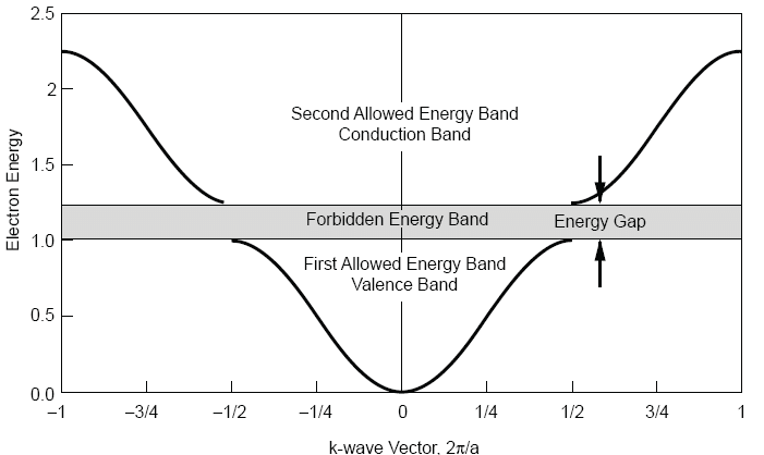
Canvas 3 shows the mode wave plot along with the potential function. Both of these functions are periodic but usually with different periods. When the mode number is the one where the band gap occurs, the period of the wave for that mode number is about twice the period of the cosine potential. In fact, in quantum physics, the mode number is the number of nodes (zeros) of the Schrodinger equation (or quantum) wave. The wave Vs mode number alternates between even (symmetric) and odd (antisymmetric) as the mode number increases. Since the cosine potential is even with respect to the center of the potential well, it is easy to see that the wave alternates between even and odd with respect to the cosine potential. The learner should notice that, when the chosen wave vector is close to the one associated with the energy at the band gap, the envelope of the wave vector becomes bell shaped. The envelopes of the other wave plots are reasonably flat over the width of finite energy well except at the edges where they drop off as exponentials since the wave cannot penetrate very far into the walls of the energy well. The reason for the large change in charactor of the wave at the energy gap is easily seen if one forms the integral associated with the perturbation effect of the cosine potential. For a wave that is even with respect to the center of the well (a cosine wave) we have:
`deltaE=int_-oo^oocoskxcosk_Vxcoskxdx\ \ \ \(1)`
where `k` is the Schrodinger wave vector and `k_V`is the wave vector associated with the potential energy. On the other hand, for a wave that is odd with respect to the center of the well (a sine wave) we have`deltaE=int_-oo^oosinkxcosk_Vxsinkxdx\ \ \ \ (2)`
Note that`cos^2(kx)=(1+cos(2kx))/2\ \ \ \ (3)`
while`sin^2(kx)=(1-cos(2kx))/2\ \ \ (4)`
The unity terms in equations 3 and 4 integrate to zero since the average value of `cosk_Vx` is zero. Then equation 1 results in a larger `deltaE` than equation 2 because of the difference between even and odd wave functions. This might appear to explain the band gap in a very simple manner but it would mean that the wave functions for energies above the band gap would all have to be even and the wave functions for energies below the band gap would all have to be odd. It is easy to see that the wave function symmetry continues to alternate between even and odd at all mode energies. So low order perturbation integrals cannot explain the band gap and we conclude that solving for the eigensystem as we have done above is the most viable means of getting the correct results. It is easy to see that the integrals in equations 1 and 2 become large if `k_V` equals approximately 2k i.e. `2k=k_V` condition or mode where the band gap occurs. That results in drastic changes that we see in the envelope of the wave at the mode (k vector0 where the band gap occurs.Canvas 4 plots the effective mass (blue) and the inverse of the effective mass `(d^2E)/(dk^2)` (green) When the cosine potential amplitude is zero the mode energy is proportional to the square of the mode number. This results in an effective mass of value 1 (as assumed in the Introduction) and is therefore constant with respect to mode number. When the cosine potential amplitude is not zero the value of `(d^2E)/(dk^2)` is sometimes less than zero, so the effective mass becomes negative so that, with a voltage applied, electron current is opposite its usual direction.
If you examine the band diagrams versus direction, you will notice that there is a continuous energy variation between the directions of the principal lattice planes. These variations in the band gap are due to the change, with electron incidence angle, `theta`, in spacing in the lattice planes. The effective lattice spacing becomes `acostheta` which causes all of the mode energies as well as the band gap to be increased by the factor `1/costheta`
This uses QR decomposition of the finite difference matrix that represents the Schrodinger equation for the given potentials. The energies, after many iterations, nIts, are on the diagonal of the R*Q matrix and the eigenvectors are in the columns of the `Q_iprod(Q_j)` matrix. See function iterateVectors(FDM,nIts) in the defVariables.js file.
`N_i=sqrt(N_cN_v)exp(-(E_g)/(2kT))`
where `N_c` is the conduction band density of states and `N_v` is the valence band density of states, `Eg` is the energy gap and `kT=0.026 eV` is the particle thermal energy at 300K. Silicon with a band gap of 1.14 electron volts, has `N_i=1.5x10^21` per `"meter"^3`. Now the builtin voltage across a diode has equation:
`V_(bi)=k_BTln((N_AN_D)/N_i^2)=k_BTln[(N_AN_D)/(N_cN_v)]exp((E_g)/(kT))]=E_g+k_BT[(N_AN_D)/(N_cN_v)]`
I hope that the reader finds that this document supplies that demonstration.